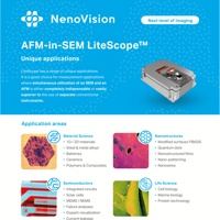
• LiteScope™
    • Main benefits
    • Why AFM in SEM?
    • Correlative microscopy
    • LiteScope package
    • Measuring modes
    • Accessories
    • SEM integration
  • Applications
    • Material science
    • Nanostructures
    • Semiconductors
    • Life science
  • About us
    • Company
    • News
    • Recommendations
    • Articles
    • Projects
  • Support
    • Webinars
    • Videos
    • Application notes
    • Product lists
    • Conference materials
  • Partners
  • Contact
  • Jobs
  • NenoVision
  • Applications

Applications

Explore the next level of correlative microscopy

Choose your application field

Characteristics of materials such as their structural, mechanical, chemical, electrical, and magnetic properties Material science
In-situ analysis of special applications such as surface modification, failure analysis, and surface chemical analysis Nanostructures
AFM-in-SEM approach in semiconductor manufacturing, failure analysis, research, and development. Semiconductors
Measurements on biological samples at the nanoscale that are difficult or even impossible using separate imaging modalities Life science

Do you have more questions?
contact us

Subscribe to our newsletter
Stay up to date and receive the latest news

Subscribe

Company address

NenoVision s.r.o.

Purkyňova 649/127
612 00 Brno
Czech Republic
VAT: CZ04525671

Contact

info@nenovision.com

Facebook LinkedIn Twitter

© 2021 - NenoVision s.r.o.

Newsletter subscribe

By signing up you agree to the terms of service.