Cutting-edge CPEM technology allows the simultaneous acquisition of AFM and SEM data and their seamless correlation.
In-situ conditions inside the SEM ensure sample analysis at the same time, in the same place and under the same conditions.
Extremely precise and timesaving approach uses SEM to navigate the AFM tip to the region of interest, enabling its fast & easy localization.
The complex sample analysis at nanoscale is the crucial point in the research process. However, the need for multiple analytical instruments to undertake the correlative analysis was complicating the overall measurement feasibility.
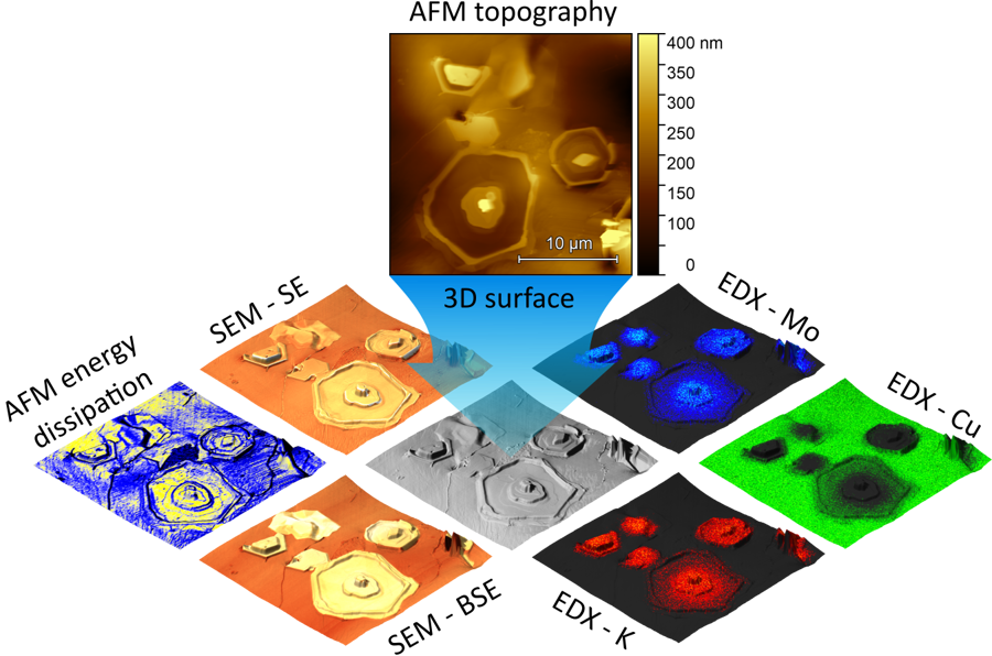
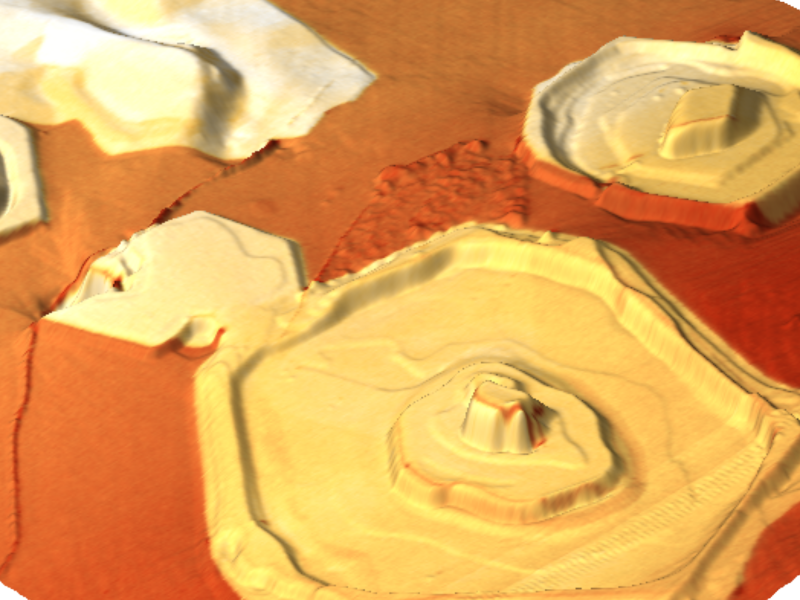
The introduction of the AFM-in-SEM technology via LiteScope changed this situation. Its unique method of multidimodal imaging (CPEM) enables simultaneous acquisition of the data from SEM and AFM, and their seamless correlation into 3D images. Thanks to LiteScope, you can correlate sample topography, mechanical, electrical, chemical and magentic properties.
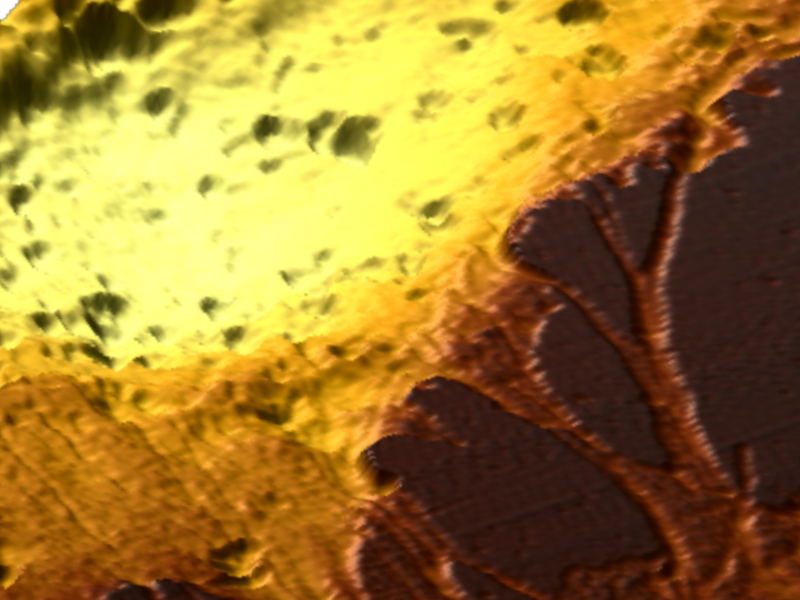
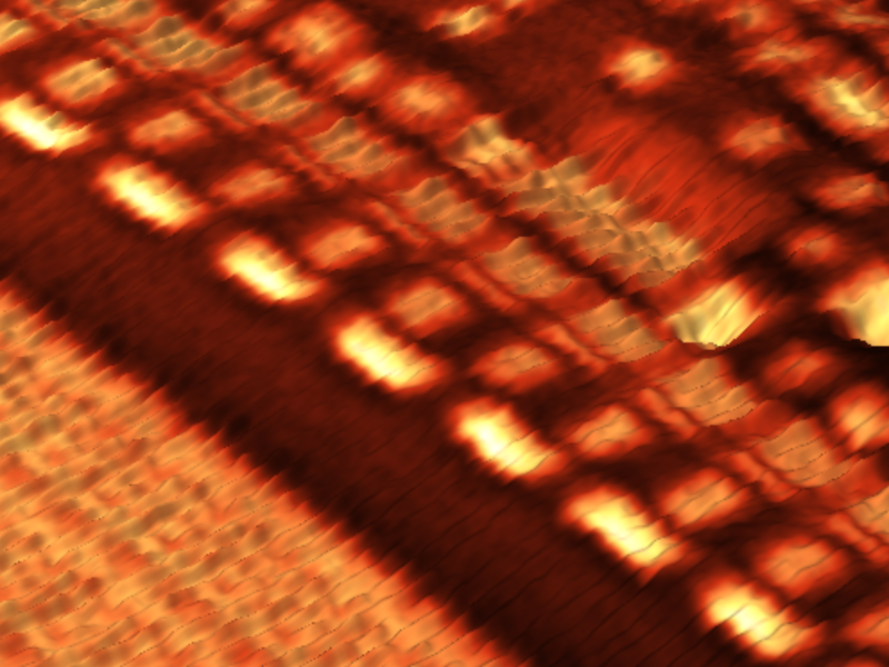
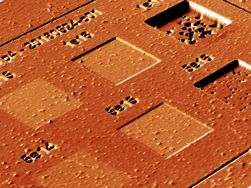
On the image on the left you can see an example of the broad spectre of channels acquired during LiteScope measurement. All of these AFM and SEM channels were acquired in in-situ conditions and their immediate correlation in our NenoView software offers a unique complex information about different properties of the sample.
The need of in-situ analysis of sensitive samples was one of the principal impulses for designing the AFM-in-SEM LiteScope. Thanks to our innovative setup, it's finally possible to perform both AFM and SEM analysis directly in the SEM chamber without exposure to ambient conditions. That means no risk of sample contamination.
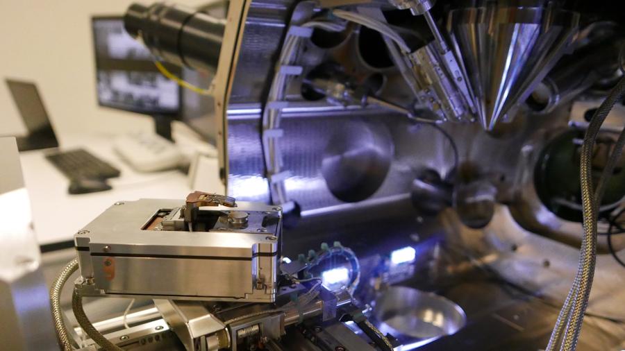
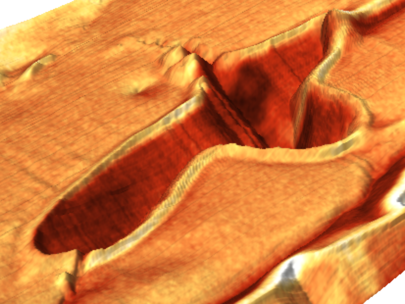
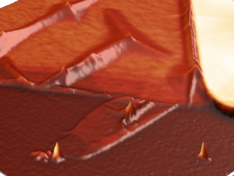
As you can see on the picture on the left, LiteScope installed in the SEM chamber makes possible to measure in-situ induced sample modification and analysis of changes, be it mechanical, electrical, chemical or any other. All the measurements can be done at the same time, in the same place and under the same conditions.
Extremely precise and time-saving approach uses SEM to navigate the AFM tip to the region of interest, enabling its fast & easy localization.
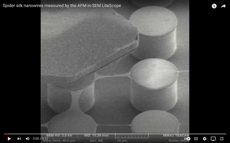
A nice example can be seen on the video on the left, showing that we were able to guide the AFM tip precisely to such a tiny nanostructure as spider silk wires.
In general, the principal problem while using separate AFM and SEM instrumentation occurs during the sample transfer between both instruments. In this case, it's nearly impossible to navigate the AFM tip to the sample spot previously measured in the SEM.
With LiteScope, you don't have to waste your precious time while trying to find that spot with your AFM tip. You'll leverage our quick & straightforward solution!
Want more info? Feel free to...

LiteScope Featured in a Nanoscale Study on Back-Contact-Free Electrical AFM
A new study in Nanoscale introduces electron-beam excited AFM (EB-AFM) — a way to run electrical AFM without a physical back-contact. A low-energy electron beam near the AFM probe acts as a remote electrode, removing the destructive sample preparation that conventional conductive AFM requires.

LiteScope Helps Localize Defects Invisible to SEM in a Joint Study with NVIDIA
A study presented at ISTFA 2025 by NVIDIA and NenoVision introduces a streamlined approach to semiconductor failure analysis. The work integrates in-situ conductive AFM (CAFM) with plasma FIB in a single SEM platform, making it possible to localize electrical defects that conventional SEM imaging can miss.

LiteScope Contributes to Study on Creep Behavior and Microstructure Evolution in Advanced Alloys
A recent study published in the Journal of Materials Science investigates the microstructural evolution and creep behavior of recrystallized FeCr-based alloys. The work combines multiple correlative microscopy techniques to provide a comprehensive view of grain structure, crystallite size, and surface topography.