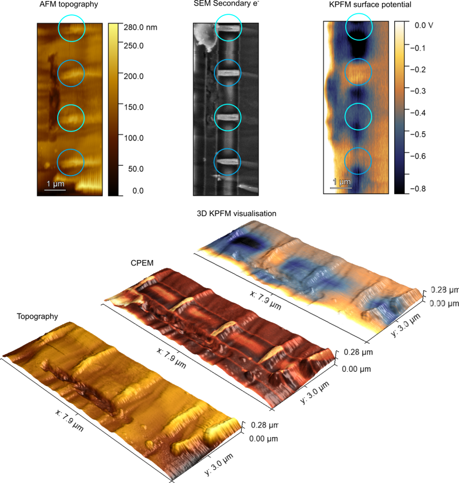
Precise analysis of defects is crucial in the production and characterisation of semiconductorsmultimodal analysis on a nanoscale. Therefore, in-situ multimodal analysis on a nanoscale level is of high interest.
For example, polished tungsten plugs in a cross-section of CMOS-type chips were simultaneously analysed by AFM, SEM and KPFM techniques. The measurement showed that the contact potential of the pins alternates between two values.
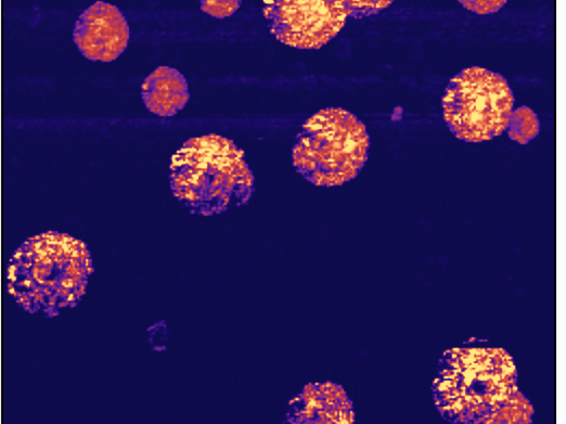
Measurement modes: KPFM, Topography
LiteScope benefits:
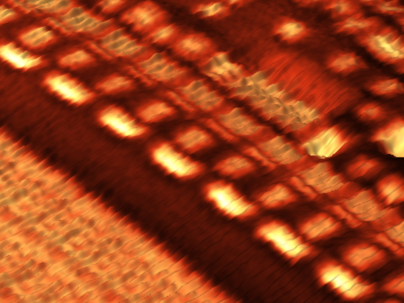
- Correlated AFM, KPFM and SEM analysis
- Easy localisation to the region of interest
- Essential for fabrication and functionality of semiconductor structures
Sample courtesy of Michael Walther, X-FAB
Want to discuss your own application?