Unique Atomic Force Microscope LiteScope is designed to merge the strengths of AFM and SEM techniques, resulting in effective workflow and extending the possibilities of correlative microscopy and in-situ analysis that ware difficult or almost impossible by conventional instrumentation.
- In-situ multimodal & correlative analysis
- Optimized & time-efficient workflow
- Ultimate performance inside SEM
- Open-hardware design for easy customization
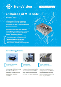
Cutting-edge CPEM technology allows the simultaneous acquisition of AFM and SEM data and their seamless correlation.
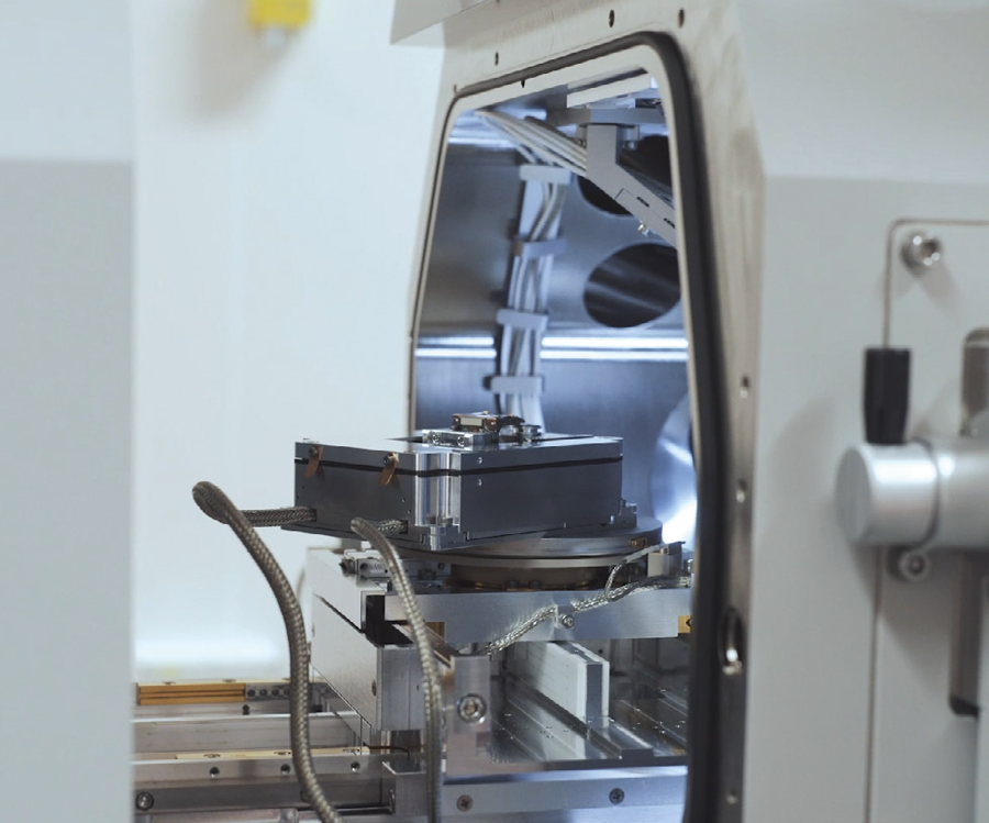
In-situ conditions inside the SEM ensure sample analysis at the same time, in the same place and under the same conditions.
Extremely precise and timesaving approach uses SEM to navigate the AFM tip to the region of interest, enabling its fast & easy localization.
Novel method of correlative imaging
Complex, yet time-efficient analysis via Correlative Probe and Electron Microscopy (CPEM) allows 3D correlative imaging that eliminates the need for repetitive tasks previously required to achieve similar kind of results.
All-in-one solution for automated in-situ analysis of multiple material properties enables unique combination of data such as topography, material contrast, mechanical or electrical properties resulting in three dimensional CPEM images.
Complex in-situ characterisation
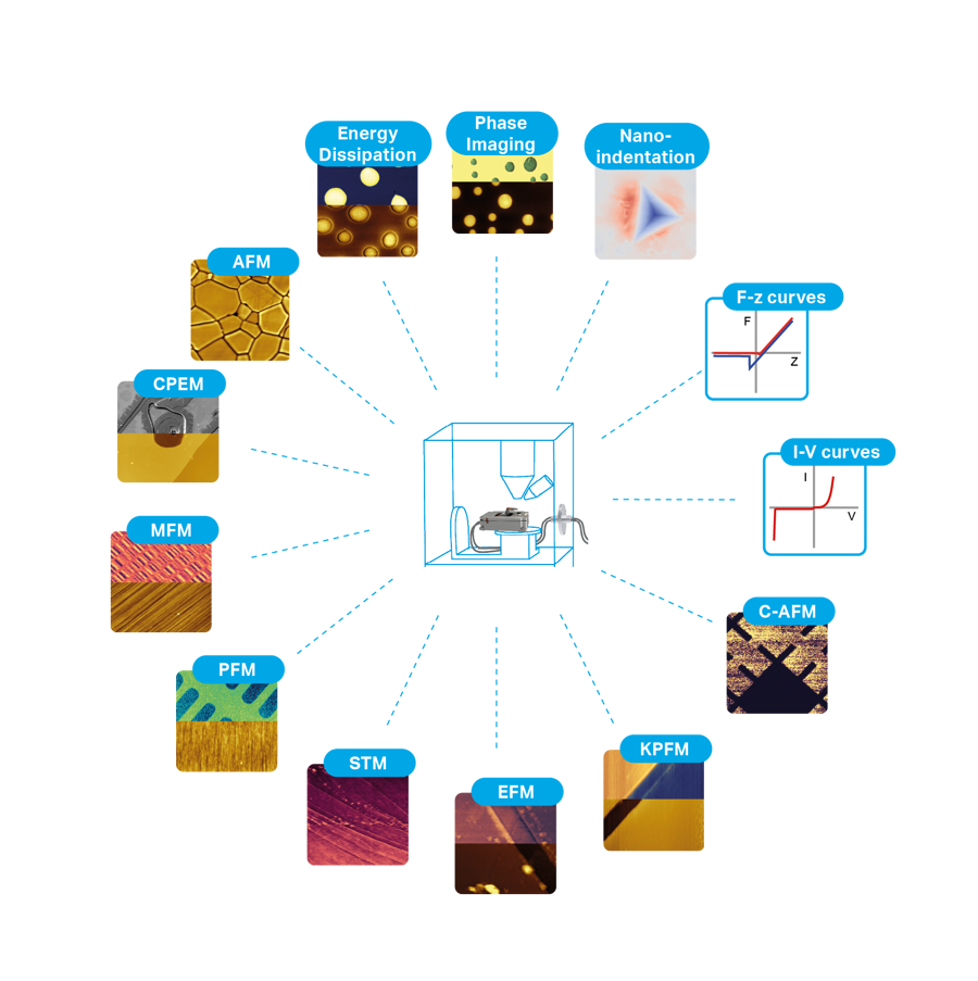
AFM brings new inside-to-SEM method of characterisation, enabling the analysis of a broad range of properties:
Material mechanical properties
- topography
- local elastic properties (tapping & contact mode)
- local sample hardness (non-topographic)
- depth-dependent material characterization
- various in-situ operations
Material magnetic properties
- magnetic domain imaging
Material electro-mechanical properties
- piezoelectric domain imaging
Material electrical properties
- conductivity map (including insulated areas)
- local surface potential
- local electrical properties (non-topographic)
- sub-nanometer topography
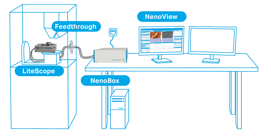
Installation package:
- LiteScope – scan head
- NenoBox – control unit
- NenoView – control software
- SEM adaptation plate
- Vacuum feedthrough
- Cabling
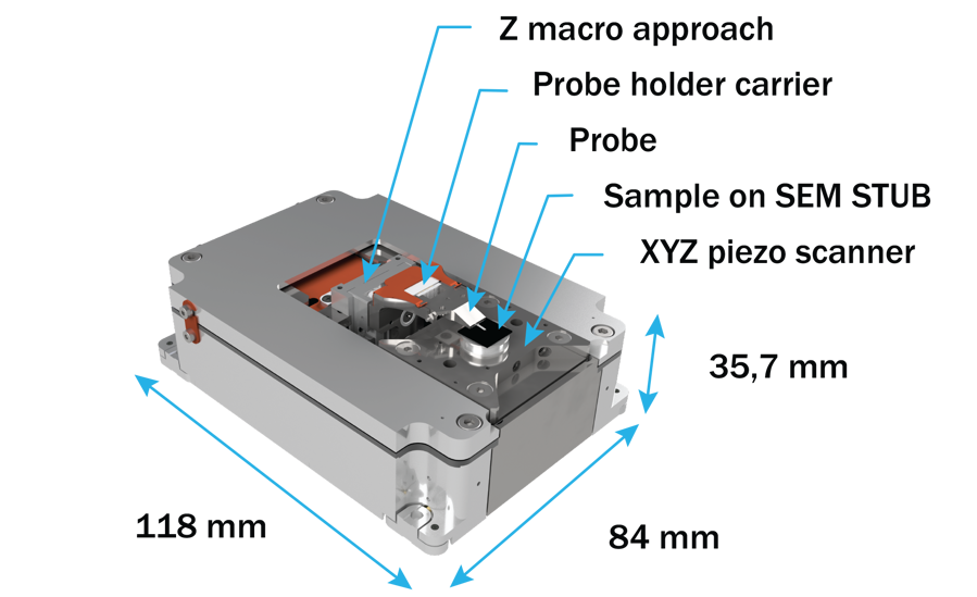
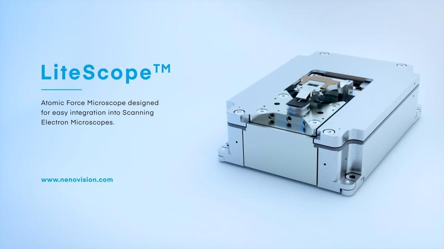
LiteScope - scan head
LiteScope is an AFM designed for fast and easy integration within SEM (operational as a standalone AFM as well).
Supports Correlative Probe and Electron Microscopy technology (CPEM).
- Comprehensive surface characterization – material mechanical, magnetic, electro-mechanical and electric properties
- Compact design compatible with most SEM systems
- Easy SEM mounting or removal in less than five minutes
- Compatible with FIB, GIS, EDX, and other accessories
- Self-sensing probes without optical detection or laser adjustment
- Special accessories and modules
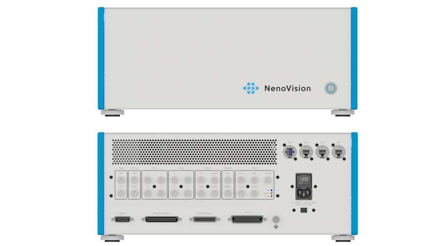
Nenobox - control unit
NenoBox integrates all the electronics necessary for running LiteScope inside of your SEM. Thanks to this unit you can measure with all the available techniques which LiteScope offers, with no need for any external devices.
Whole NenoBox is based on the open-hardware concept, enabling its modifications by customers to enhance its versatility. It was developed in cooperation with our partners from the Czech Metrology Institute and based in their advanced GwyScope DSP controller. Thanks to this cooperation, we can offer full development support for all the curious scientists using LiteScope!
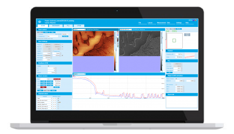
NenoView - control software
Online-based NenoView software offers a wide range of features that assure time-efficient and easy work with LiteScope AFM-in-SEM:
- Web-based interface with remote access to user data
- Intuitive UI adaptable to customer’s needs
- AI-driven topographic correction
- Method-based automated probe tuning
- Single-click operations eliminating repetitive tasks
- AFM and SEM multichannel data aquisition
- Schematics of device configuration
- Possibility of measurement control via inbuilt scripting features Compatible with Gwyddion or MountainsSPIP software for further data postprocessing
Are you interested? Feel free to...

LiteScope Phenom now live with Aptco Group

Where to Meet NenoVision in 2026: Five Conferences Across Three Continents

From Brno to Taiwan: LiteScope Meets the Heart of the Semiconductor World
