

LiteScope Featured in a Langmuir Study on Operando Work-Function Imaging of Catalytic Reactions
A new study in Langmuir combines operando SEM with Kelvin probe force microscopy (FM-KPFM) to image, for the first time, the work function of a catalyst surface while a chemical reaction is actually happening on it.

LiteScope Featured in a Nanoscale Study on Back-Contact-Free Electrical AFM
A new study in Nanoscale introduces electron-beam excited AFM (EB-AFM) — a way to run electrical AFM without a physical back-contact. A low-energy electron beam near the AFM probe acts as a remote electrode, removing the destructive sample preparation that conventional conductive AFM requires.

LiteScope Helps Localize Defects Invisible to SEM in a Joint Study with NVIDIA
A study presented at ISTFA 2025 by NVIDIA and NenoVision introduces a streamlined approach to semiconductor failure analysis. The work integrates in-situ conductive AFM (CAFM) with plasma FIB in a single SEM platform, making it possible to localize electrical defects that conventional SEM imaging can miss.

LiteScope Contributes to Study on Creep Behavior and Microstructure Evolution in Advanced Alloys
A recent study published in the Journal of Materials Science investigates the microstructural evolution and creep behavior of recrystallized FeCr-based alloys. The work combines multiple correlative microscopy techniques to provide a comprehensive view of grain structure, crystallite size, and surface topography.
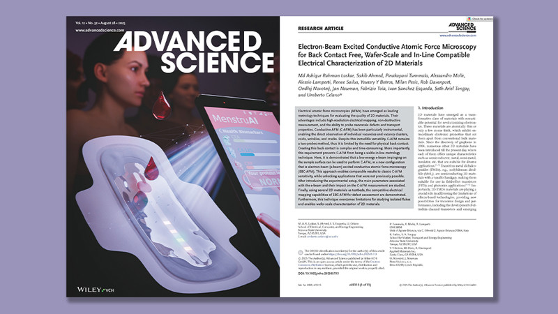
LiteScope Featured in a Breakthrough Study on Electron-Beam-Excited Conductive AFM
A new study has succesfully demonstrated Electron-Beam-Excited Conductive AFM (EBC-AFM) on semiconductive 2D materials – an approach that removes the need for back-contact and time consuming sample manipulation required with traditional conductive AFM. Instead, the SEM’s electron beam generates charge carriers that close the circuit with the AFM tip, making it possible to carry out fast, non-destructive electrical mapping of 2D materials, including full wafers.
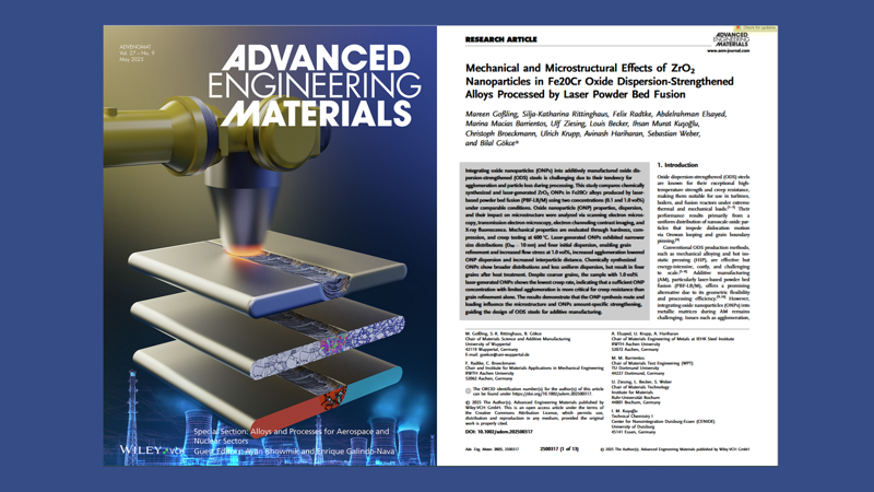
ZrO2 Nanoparticles in Fe20Cr Oxide Dispersion-Strengthened Alloys Processed by Laser Powder Bed Fusion
The study investigates oxide nanoparticles (ONPs), specifically ZrO2 nanoparticles in Fe20Cr alloys, produced via laser powder bed fusion (PBF-LB/M), in order to understand how these nanoparticles impact the microstructure and mechanical properties. LiteScope was used for validating Electron Channeling Contrast Imaging (ECCI) findings and to distinguish nanoparticles (ONPs) from pores or preparation artifacts.





Want to ask more? Feel free to…