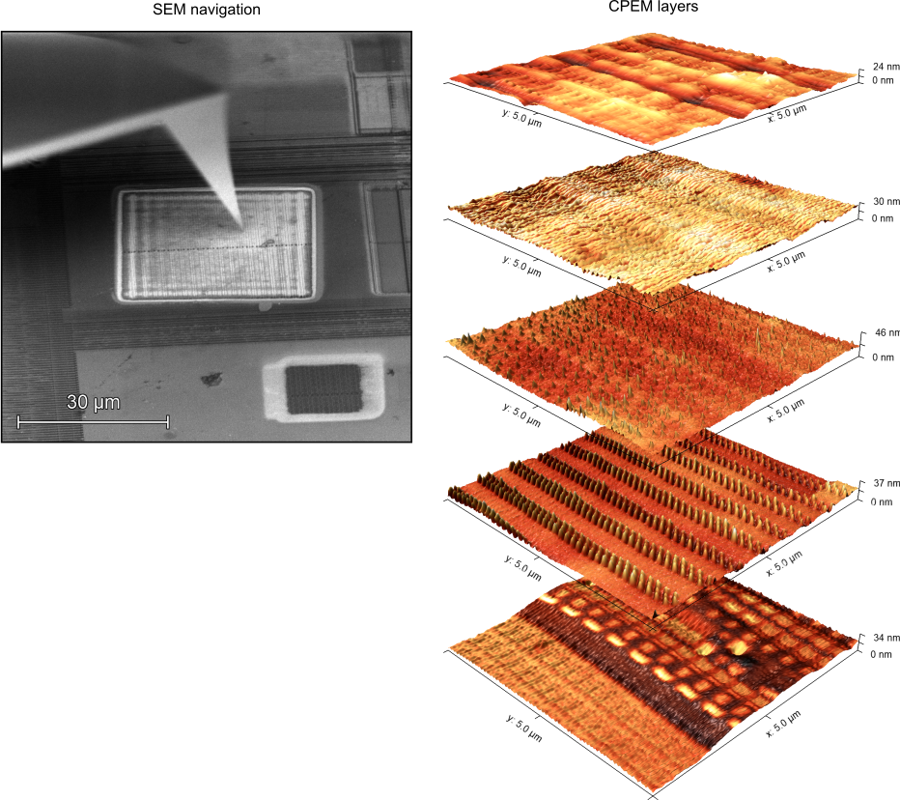
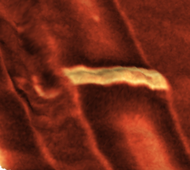
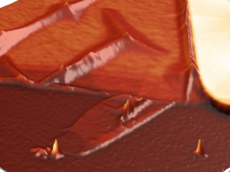
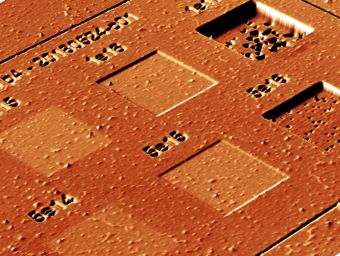
Due to miniaturization, failure analysis of advanced integrated circuits is possible only by local-focused ion beam (FIB) delayering. Diminution of FIB polishing artifacts such as curtaining or delayered surface roughness is crucial for the comprehension of the failures at the nanoscale dimension.
Using AFM-in-SEM technology, we were able to perform in-situ multi-modal study of integrated circuits subsequently after their FIB treatment.
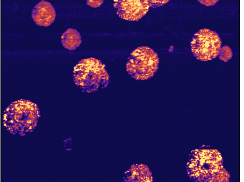
Measurement modes: Topography
LiteScope benefits:
- In-situ sample analysis by multiple techniques (SEM, AFM) – minimal sample damage
- 3D reconstruction and roughness measurement
- Planarity control of milled structure (height profile)
Sample courtesy of Marek Šikula, TESCAN
Want to discuss your own application?