LiteScope Featured in a Breakthrough Study on Electron-Beam-Excited Conductive AFM
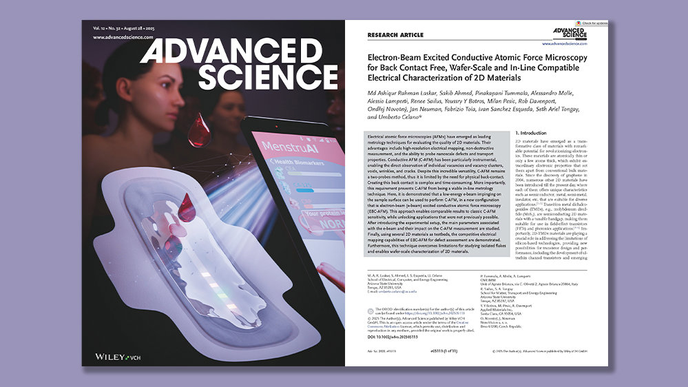
A new study has succesfully demonstrated Electron-Beam-Excited Conductive AFM (EBC-AFM) on semiconductive 2D materials – an approach that removes the need for back-contact and time consuming sample manipulation required with traditional conductive AFM. Instead, the SEM’s electron beam generates charge carriers that close the circuit with the AFM tip, making it possible to carry out fast, non-destructive electrical mapping of 2D materials, including full wafers.
Scientific articles
|
02. 09. 2025
|
by Advanced Science
Material Science
Related articles

Scientific articles
|
09. 09. 2025
|
by Journal of Materials Science
LiteScope Contributes to Study on Creep Behavior and Microstructure Evolution in Advanced Alloys
Material Science
Scientific articles
|
21. 05. 2025
|
by Advanced Engineering Materials
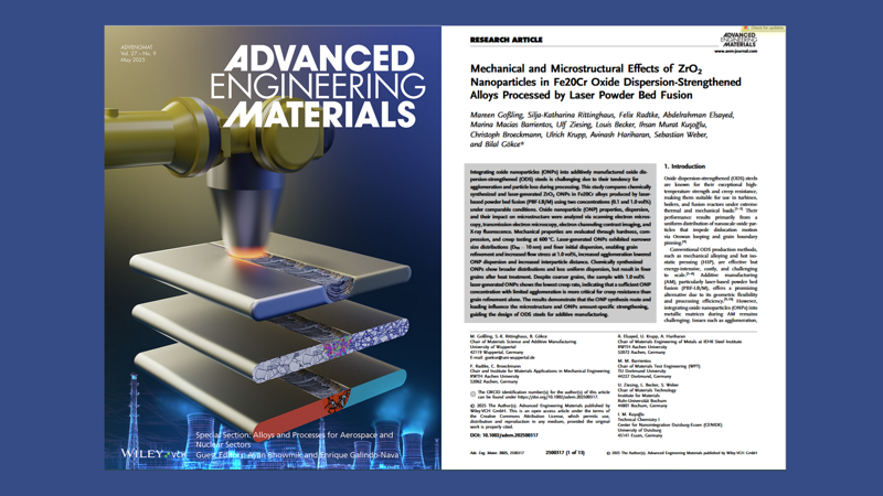
ZrO2 Nanoparticles in Fe20Cr Oxide Dispersion-Strengthened Alloys Processed by Laser Powder Bed Fusion
Material Science
Technology
Scientific articles
|
12. 03. 2025
|
by Phys. Status Solidi A
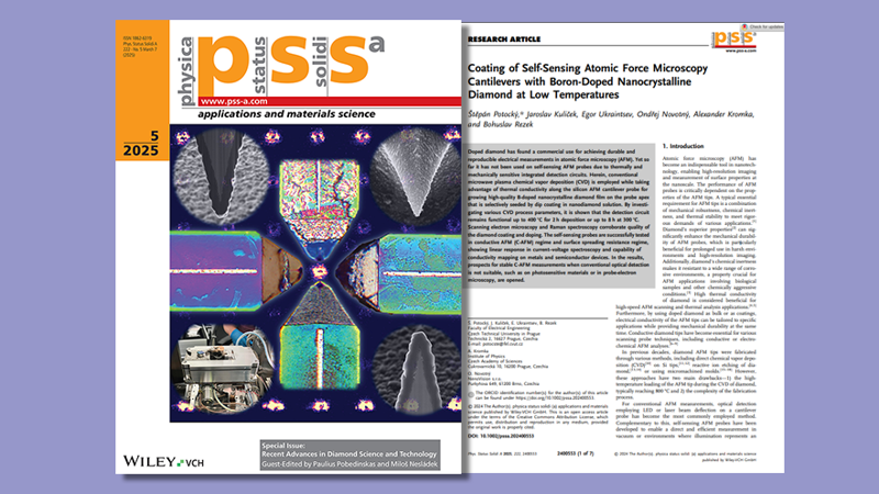
AFM-in-SEM LiteScope on the Cover of a Key Study on Diamond-Coated Probes
Material Science
Technology
Scientific articles
|
17. 12. 2024
|
by ACS Applied Electronic Materials
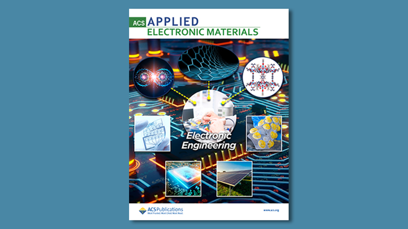
Impact of Electron Irradiation on WS2 Nanotube Devices
Material Science
Technology
Scientific articles
|
18. 11. 2024
|
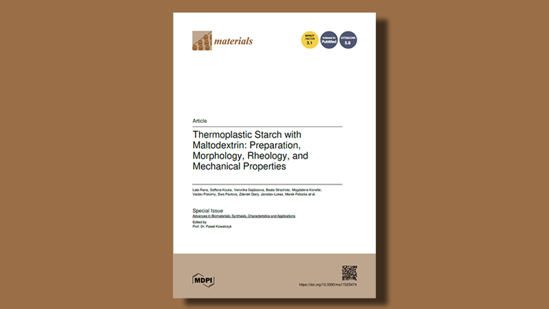
by Materials
Enhancing Thermoplastic Starch with Maltodextrin: Key Properties and Performance Insights
Material Science
Technology
