New application note: Analysis of FIB etched nanostructures
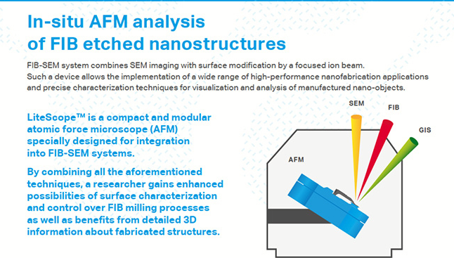
We are happy to inform you that we have prepared a new application note for you. Its name is In-situ AFM analysis of FIB etched nanostructures. Read about the key LiteScope™ advantages for FIB applications!
Publication
|
14. 11. 2019
|
by Markéta Eliášová
Nanostructures
Related posts

Product
|
12. 07. 2026
|
by Andrea Karas
LiteScope Phenom now live with Aptco Group
Product

Event
|
25. 06. 2026
|
by Andrea Karas
Where to Meet NenoVision in 2026: Five Conferences Across Three Continents
Technology

Other
|
14. 05. 2026
|
by Andrea Karas
From Brno to Taiwan: LiteScope Meets the Heart of the Semiconductor World
Semiconductors

Event
|
05. 11. 2025
|
by Sabina Žilková
NenoVision has won the Czech Head 2025 award!
Nanostructures
Semiconductors
Product
Technology

Event
|
09. 10. 2025
|
by Jana Levá
ISTFA 2025
Semiconductors
Product
Technology