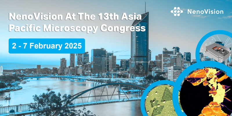
Our maximum goal is to be close to our customers & their needs. For this reason and as part of excellent collaboration with our partner institutions, we decided to certificate selected workspaces around the world as our reference laboratories. From now onwards, it will be possible to perform there live AFM-in-SEM demonstration & customer measurements for interested subjects.
Get to know the first laboratories of this type that were inaugurated to garantize an easy access to live AFM-in-SEM in-situ correlative measurements to all the interested researchers that will appreciate help of our cutting-edge technological solution. If you are interested in experiencing live AFM-in-SEM measurement in your closest laboratory, don't hesitate to contact us or the respective laboratory staff to organize your personalized measurement.
See the list of laboratories with contacts below!
My team has long championed the convergence of analytical techniques for intricate material characterization in nanoelectronics. We found LiteScope to be the perfect embodiment of this philosophy. It seamlessly integrates electrical atomic force microscopy with electron and ion microscopies, all within a pristine high-vacuum environment. This empowers us to conduct comprehensive, correlative studies of devices and materials properties, while unlocking versatile in-situ ion beam milling and deposition for sample preparation. We're thrilled to be working with the NenoVision team in pushing the boundaries of this platform and uncovering its full potential in the realm of emerging nanoelectronics.

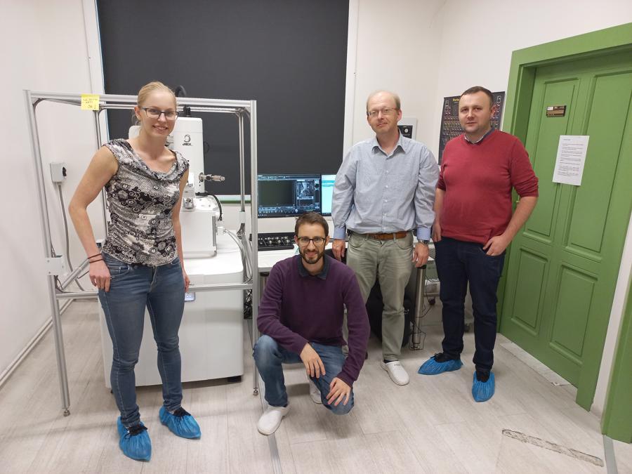
We have recently acquired the NenoVision AFM. This AFM is running inside the chamber of one of our SEMs and it enables us to do a correlative study of all materials. We can combine whatever we see in the SEM with whatever the AFM delivers. There are so many things you can do with such an AFM. It's like having a Swiss army knife inside the chamber of your SEM.

Jan Neuman provided an impressive talk at the E-MRS European Nanoanalysis Symposium 2020. He presented numerous examples of correlative microscopy applying NenoVison's AFM-in-SEM system. Considering the wide range of measuring modes this system is offering, NenoVision will open the door to correlative materials characterization. I am convinced that researchers in Physics, Chemistry, Materials Science, and Life Science will benefit from this innovative product.

We have greatly appreciated every aspect of our collaboration with NenoVision. Our communication has been smooth, efficient, and informative. By utilizing their novel CPEM technology, NenoVision helped us gain unique 3D information about our nano-sized samples deposited on cm-sized substrates. The unique ability to utilize both SEM and AFM at the same time allowed us to directly correlate the size and mechanical properties of silk nanowires. We truly appreciated all the assistance we received from NenoVision and hope to continue this fruitful collaboration in the future.

I would like to thank for the assistance that I am receiving at NenoVision for the development of my research. The extraordinary level of expertise and scientific knowledge that I found there is fundamental for my project and the high quality of the imaging obtained with LiteScope has produced outstanding results so far. I hope to keep continuing my collaboration with NenoVision also in the future.
We implement the AFM in SEM technology in the field of low dimensional materials research. The correlative AFM in SEM microscopy embodied in LiteScope opens up a brand new dimension of knowledge about these materials' properties and their optimization.

In my research, LiteScope more intuitively reflected the 3D surface morphology of the composite film. In addition, if the characterization of the morphology and electrical properties of the composite films will be combined and measured at the same time, it will bring a more convenient solution for solar cells related research.

We just got our LiteScope and are really excited about new possibilities to perform in-situ AFM investigations on our materials. Many thanks to Radek Dao and Radek Řihák for their incredible professional performance by the installation. They finished an immense amount of work in two days, and we couldn't be happier with the result. Also, many thanks to David Novák for the excellent coordination. Working with the team of NenoVision was a pleasure.

LiteScope is a true extension of horizons in the field of material engineering and semiconductors. I appreciate the innovative approach of its creators who were not afraid to look at AFM technology from a different perspective. I am honored that our institute has a serial number 01.

NenoVision is a good example of bringing together academic and business spheres. The unique idea of students has been transformed into a world patent LiteScope that has the chance to disturb the waters of nanoscience. It is pleasing to use the knowledge gained through this invention in international projects.
I have had the pleasure of working with the NenoVision team. Application of their unique imaging technology, i.e. the Correlative Probe and Electron Microscopy (CPEM), enables us to progress our research in the field of characterization of the secondary phases in advanced high strength steels and provides a novel insight into multiphase steels structures. The CPEM technique is a powerful tool for the investigation of complex steels and opens the door to a better understanding of the structure-mechanical properties relationship. I with full confidence recommend NenoVision as a professional and reliable research partner.
Using LiteScope's technique allowed us to describe the formation of blisters on the surface of highly oriented pyrolytic graphite during the atomic layer deposition process. Easy localization of the area of interest using the SEM and following local characterization of the surface by the AFM provided us with topographical information about blistered features and their behavior in a vacuum and in air. Special thanks go to the specialists from NenoVision for the consultation, help, and training.

The integration of LiteScope into the scanning electron microscope enables us to precisely characterize the topography of areas invisible to the human eye or to the light microscopes. The correlation of the AFM and SEM signals acquired simultaneously in the same area enabled us to identify the relationship between extensive defects in III-Nitride semiconductors and their conductivity.

Combining SEM imaging under various acceleration voltages and regimes (SE, BSE) with atomic force microscopy at the same spot has proven highly valuable in our Life Science research of interactions between bacteria and various nanomaterials. For instance, only by combining the SEM and AFM techniques we obtained correct insight into the properties and interaction of diamond-metal composite nanoparticles and E. Coli bacteria. Collaboration with Nenovision also helped us advance the methodology for precise analysis and visualization of the correlated CPEM (AFM+SEM) data on life science specimens.

Want to get in touch? Feel free to...
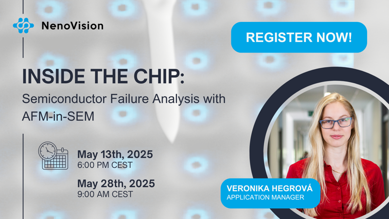
Inside the Chip: Semiconductor Failure Analysis with AFM-in-SEM
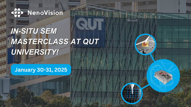
In-Situ SEM Masterclass at QUT University!
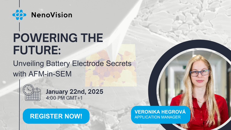
Upcoming Battery Webinar | Unveiling Battery Electrode Secrets with AFM-in-SEM