How NVIDIA Uses AFM-in-SEM to Find Defects Invisible to Conventional Semiconductor Failure Analysis

When transistors shrink to the 5nm node, standard SEM-based failure analysis starts missing defects. See how NVIDIA engineers used NenoVision's AFM-in-SEM to find what conventional tools couldn't.
This work was led by Dr. Chuan Zhang and Dr. Jane Li
from NVIDIA's Silicon Failure Analysis Lab — in collaboration
with NenoVision's Radek Dao and Rosalinda Ring.
Why Conventional Failure Analysis Falls Short at Advanced Nodes
As device geometries shrink, traditional methods lose sensitivity. SEM-based passive voltage contrast (PVC) struggles to detect electrically subtle or buried defects — and at the 5nm node, subtle is the norm.
Sample preparation adds another layer of complexity. Chemical mechanical planarization (CMP) exposes conductive structures to ambient conditions, leading to oxidation. New materials like cobalt contacts oxidize almost instantly. Every transfer between instruments — pFIB to AFM and back — means another vacuum cycle, another risk of contamination, and more time lost.
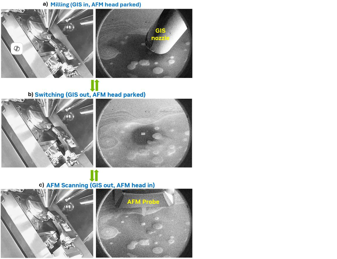
The Solution: CAFM Integrated Directly Inside the pFIB/SEM Chamber
NenoVision's compact LiteScope AFM was mounted directly onto the stage of NVIDIA's plasma FIB/SEM dual-beam system. The result: pFIB delayering, SEM imaging, and CAFM current imaging all happen inside a single vacuum chamber — without ever moving the sample.
- No vacuum cycles → pristine, oxide-free surfaces preserved for CAFM
- SEM + CAD navigation → fast and precise positioning of the AFM probe
- Seamless mode switching → significantly shorter overall analysis time
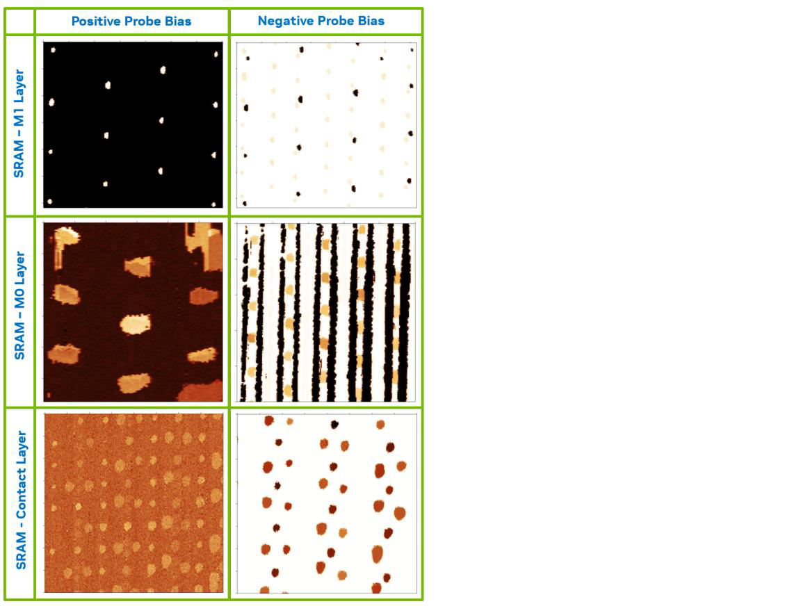
Layer-by-Layer Analysis: Logic Cells and SRAM at the 5nm Node
The team validated the workflow on a 5nm-class IC. After mechanical pre-thinning, pFIB delayering exposed individual circuit levels one by one. CAFM current imaging was performed at each level — without breaking vacuum, without re-navigating, without losing surface quality.
Case Study: Finding the Root Cause in a Stacked-Die Package
A chip in an advanced heterogeneous stacked-die package failed after electrostatic discharge testing. Initial CAFM imaging showed no anomalies — because insulating die bonding material between the stacked dies was blocking the current path.
The fix: a deep trench milled by pFIB near the suspect transistors, creating a grounding path — all within the same chamber. CAFM imaging then revealed two structures with abnormally high current. Further delayering identified two leaky gates. TEM analysis confirmed the root cause: gate oxide breakdown.
![]()
A Novel Technique: Scanning EBIC Microscopy
The integration unlocked a completely new imaging modality. By synchronizing the electron beam with the AFM probe scan, the team developed Scanning EBIC Microscopy (SEBICM) — mapping subsurface p-n junction behavior at the nanoscale, contact by contact. This goes beyond what SEM PVC or standalone CAFM can reveal.
Key Takeaways
- Faster workflow: no vacuum cycles, no manual transfers, no re-navigation
- Cleaner surfaces: oxide-free conditions maintained throughout
- Greater accuracy: SEM + CAD navigation to the exact target
- New capabilities: Scanning EBIC Microscopy for junction-level defect mapping
- Proven on real failure: gate oxide breakdown identified and confirmed by TEM
Questions?
Related posts

LiteScope Open Demo Days in Brno — Book Your Slot for May 11–15, 2026

Upcoming webinar: Challenges and Opportunities for Site-Specific Failure Analysis