From Brno to Taiwan: LiteScope Meets the Heart of the Semiconductor World

In April 2025, NenoVision's Marek Jemelka packed LiteScope and flew to Taiwan — to demonstrate AFM-in-SEM technology to top researchers, attend the first-ever EDFAS Asia Workshop, and see firsthand what it looks like when an entire country bets on semiconductors.
The Journey Begins: A Quick Stopover in Singapore
The trip started with an eight-hour layover in Singapore — just enough time to make a quick escape into the city centre, catch a glimpse of the famous Marina Bay, and reset before the main event. It was a brief but welcome reminder that science takes you to some remarkable corners of the world.
Workshop at Academia Sinica: LiteScope Live in the Electron Microscope
The first stop in Taiwan was the Institute of Physics at Academia Sinica in Taipei — one of Taiwan's most prestigious research institutions. Marek presented AFM-in-SEM technology to a room of 16 researchers, walking them through the key aspects, benefits, and applications of LiteScope and CPEM technology.
The session included a live demonstration directly inside a scanning electron microscope, showing in real time how AFM and SEM data can be acquired simultaneously and correlated at the nanoscale. For the researchers in the room, it was a chance to see the technology in action rather than on a slide.
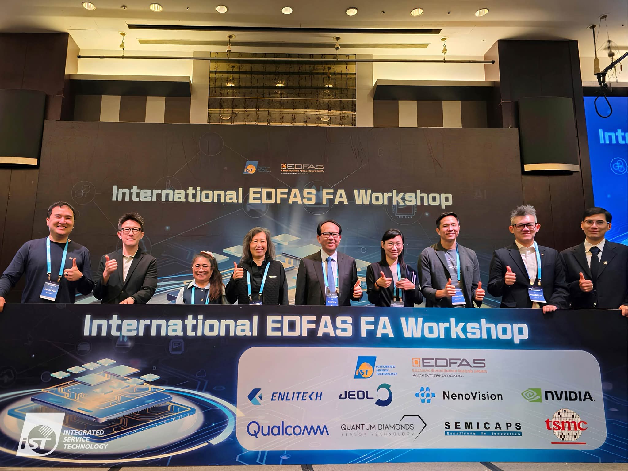
The EDFAS Asia Workshop: AFM-in-SEM Meets the FA Community
The second major event was the inaugural EDFAS Failure Analysis Workshop in Hsinchu — the first time EDFAS, the world's leading authority on electronic device failure analysis, has held an event in Asia. NenoVision was invited to present alongside industry leaders including NVIDIA, TSMC, Qualcomm, Enlitech, JEOL, and others.
Rose Ring presented LiteScope's capabilities to the advanced FA community, highlighting how AFM-in-SEM addresses some of the most pressing challenges in semiconductor failure analysis — particularly for complex packaging structures in the AI era, where conventional techniques increasingly hit their limits.
Being in that room — with the companies that define the global semiconductor industry — was a clear signal that AFM-in-SEM is no longer a niche academic tool. It belongs in the failure analysis workflow of the most demanding fabs in the world.
A Country Built on Semiconductors
Between sessions, Marek had time to absorb something that's hard to fully grasp from the outside: the sheer scale of Taiwan's semiconductor ecosystem. The Hsinchu Science Park alone is home to hundreds of companies, including the world's most advanced fabs. You can read the numbers — Taiwan produces over 90% of the world's most advanced chips — but standing in front of those facilities makes it land differently.
The story behind it is worth knowing. In the 1980s, Taiwan faced a strategic decision: how to build a world-class semiconductor industry without the capital or time to compete across the entire value chain. The answer was elegant — focus purely on manufacturing, with no end product that would compete with customers. The result was TSMC, and eventually an entire national ecosystem built around that model. Today, every major chip designer in the world sends their designs to Taiwan to be made.
What stood out compared to Europe was the relentless focus on real-world application. Taiwanese researchers and industry professionals are open about what they don't yet know, but equally determined to find the answer. There's a pragmatism and speed to the collaboration that feels different.
Taiwan Beyond the Lab
The island rises to nearly 4,000 metres - Yushan, formed by tectonic collisions, not volcanoes. And nearly every square metre that isn't built on is jungle. Every square metre that isn't built on is green. The contrast between the density of the science parks and the wildness of the landscape just beyond them is striking.
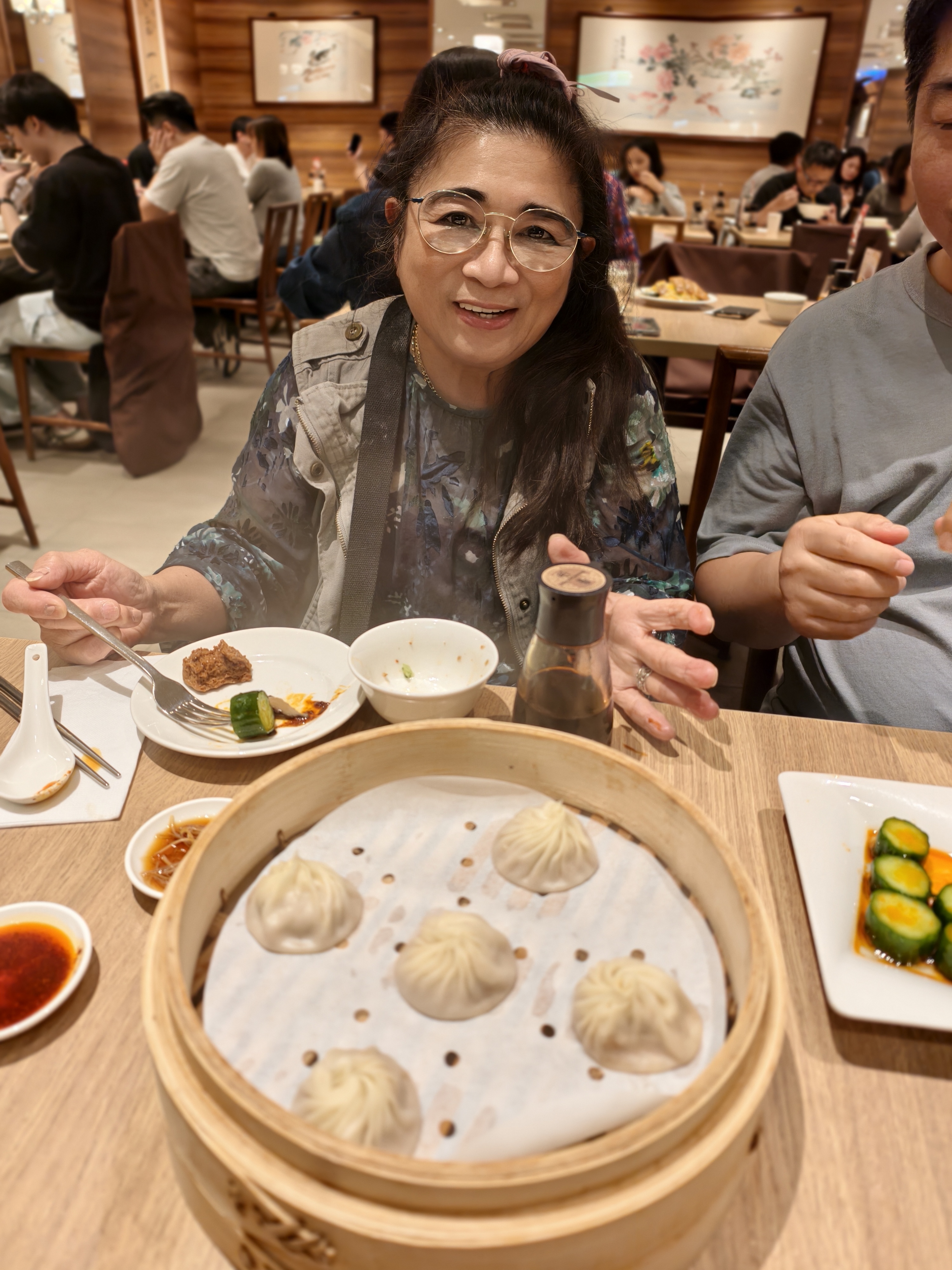
And the food. Taiwanese food culture is genuinely something else — influenced heavily by Japan, it carries with it a respect for the meal itself. Sitting down, slowing down, actually tasting what's in front of you. A good lesson for anyone used to eating on the go.
What the Trip Means for NenoVision
The Taiwan trip was more than a series of demos and presentations. It was a chance to place LiteScope in front of the people who are defining the next generation of semiconductor failure analysis — and to see, up close, the ecosystem they're working in.
The conversations started in Taipei and Hsinchu will continue. And LiteScope will be there.
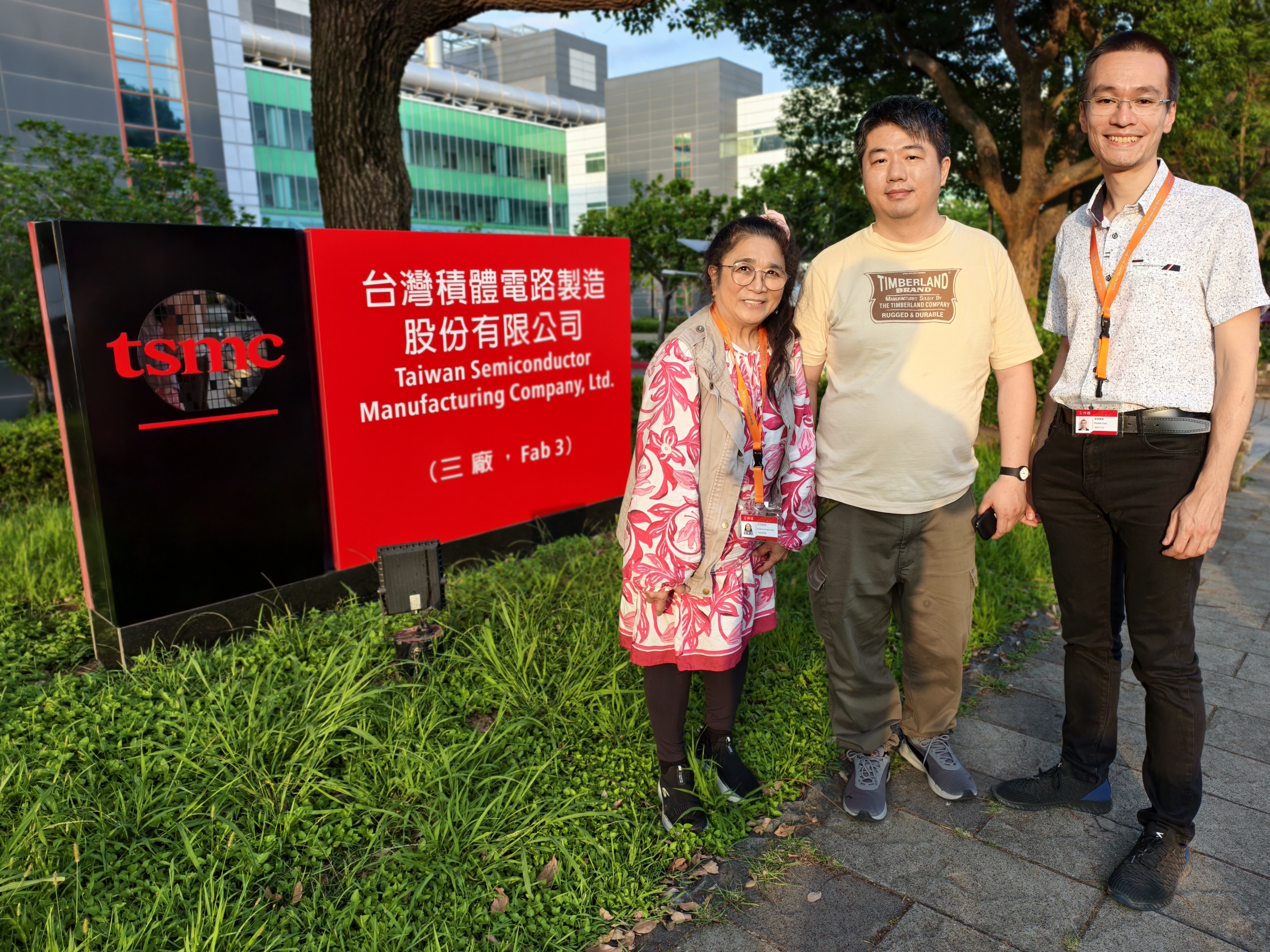
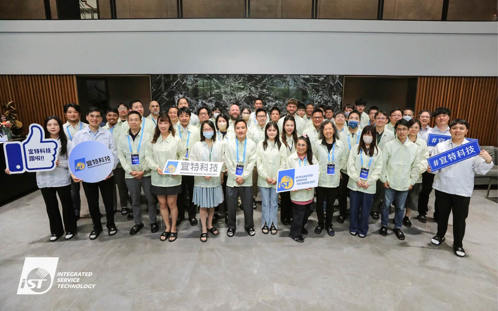
See the photos below.
Related posts

LiteScope Phenom now live with Aptco Group

Where to Meet NenoVision in 2026: Five Conferences Across Three Continents

NenoVision has won the Czech Head 2025 award!

ISTFA 2025