Workshop at Arizona State University

Workshop at Arizona State University

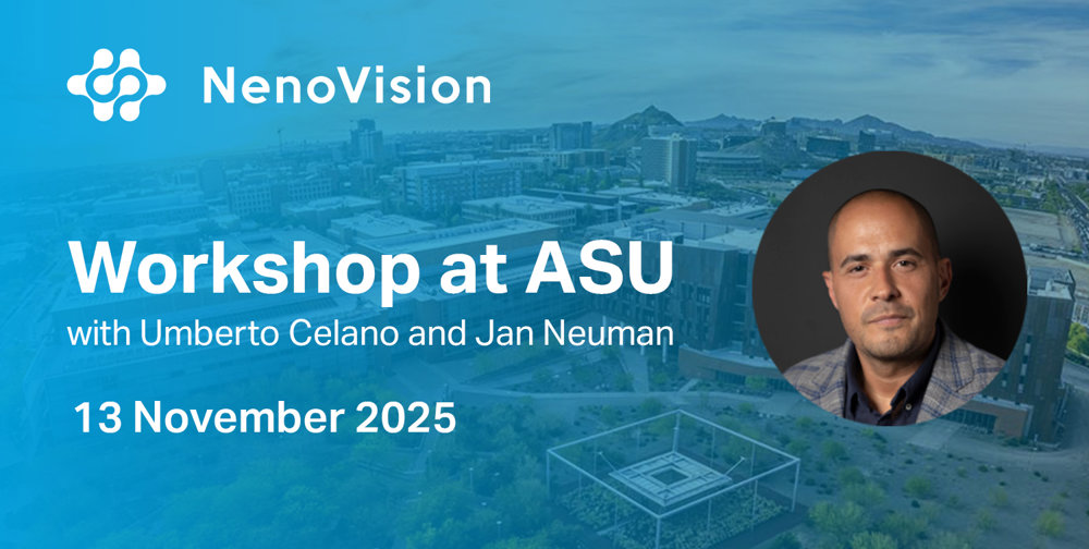
Discover LiteScope AFM‑in‑SEM at Arizona State University on 13 November 2025 with insights from Associate Professor Umberto Celano and Jan Neuman.

We are excited to announce our upcoming joint workshop on Discovering Integrated AFM-in-SEM Semiconductor Failure Analysis Flows taking place at Arizona State University on 13 November 2025.


The event will showcase LiteScope AFM-in-SEM technology with presentations by Associate Professor Umberto Celano and Jan Neuman, offering a unique opportunity to see the system in action during the live demo, gain expert insights, and connect with fellow researchers in nanoelectronics and semiconductor diagnostics.


Secure your spot today!


Registration below ↓


When?

13 November 2025


Where?

Arizona State University, USA

Tempe, Arizona

More information and the full program can be found in the flyer available for download below.


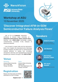
My team has long championed the convergence of analytical techniques for intricate material characterization in nanoelectronics. We found LiteScope to be the perfect embodiment of this philosophy. It seamlessly integrates electrical atomic force microscopy with electron and ion microscopies, all within a pristine high-vacuum environment. This empowers us to conduct comprehensive, correlative studies of devices and materials properties, while unlocking versatile in-situ ion beam milling and deposition for sample preparation. We're thrilled to be working with the NenoVision team in pushing the boundaries of this platform and uncovering its full potential in the realm of emerging nanoelectronics.

Umberto Celano
Arizona State University / Group Leader in Nanoelectronics Metrology & Failure Analysis Lab

What you can look forward to:

  • Learn about Nanoelectronics Metrology & Failure Analysis Lab and their research into semiconductor material behavior with in-situ electron microscopy
  • Explore AFM-in-SEM technology with Jan Neuman and understand its unique strengths in correlating mechanical, electrical, and topographical sample properties
  • Dive deeper into different applications and real case studies with LiteScope AFM-in-SEM
  • Experience a live demo of LiteScope & get all your questions answered during Q&A


Other Speakers & Abstracts

Md Jayed Hossain, Arizona State University, School of Electrical, Computer, and Energy Engineering, Tempe, AZ, 85281


Transition metal dichalcogenides (TMDs) are promising candidates for future semiconductor technologies, but their integration requires precise control over defects during growth, transfer, and device fabrication. Conductive AFM (C-AFM) is a powerful tool for nanoscale electrical characterization, yet manual interpretation is time-consuming and prone to inconsistency. We introduce a computer vision–assisted workflow that automates C-AFM data analysis, enabling rapid and objective quantification of key parameters such as defect coverage, defect density, and grain boundary length. Validated against hand-labeled datasets, the approach ensures consistency and scalability, providing a robust pathway toward standardized defect metrology and quality control in 2D semiconductors.

A novel electron-beam assisted conductive atomic force microscopy (EBC‑AFM) technique enables back-contact free electrical measurements of 2D material samples. By leveraging electron-beam excitation, the method can probe electrical properties in-line and at full wafer scale, eliminating the need for traditional metal back contacts. This approach promises high spatial resolution and throughput, making it suitable for process monitoring in industrial fabrication environments. Moreover, its compatibility with wafer-scale and in-line workflows could significantly enhance quality control and characterization speed for emerging 2D electronic devices. Overall, EBC‑AFM offers a scalable, non-destructive way to map electrical behavior in 2D materials with precision and efficiency.

ASU Workshop Registration

Form.Select.ErrorMessage