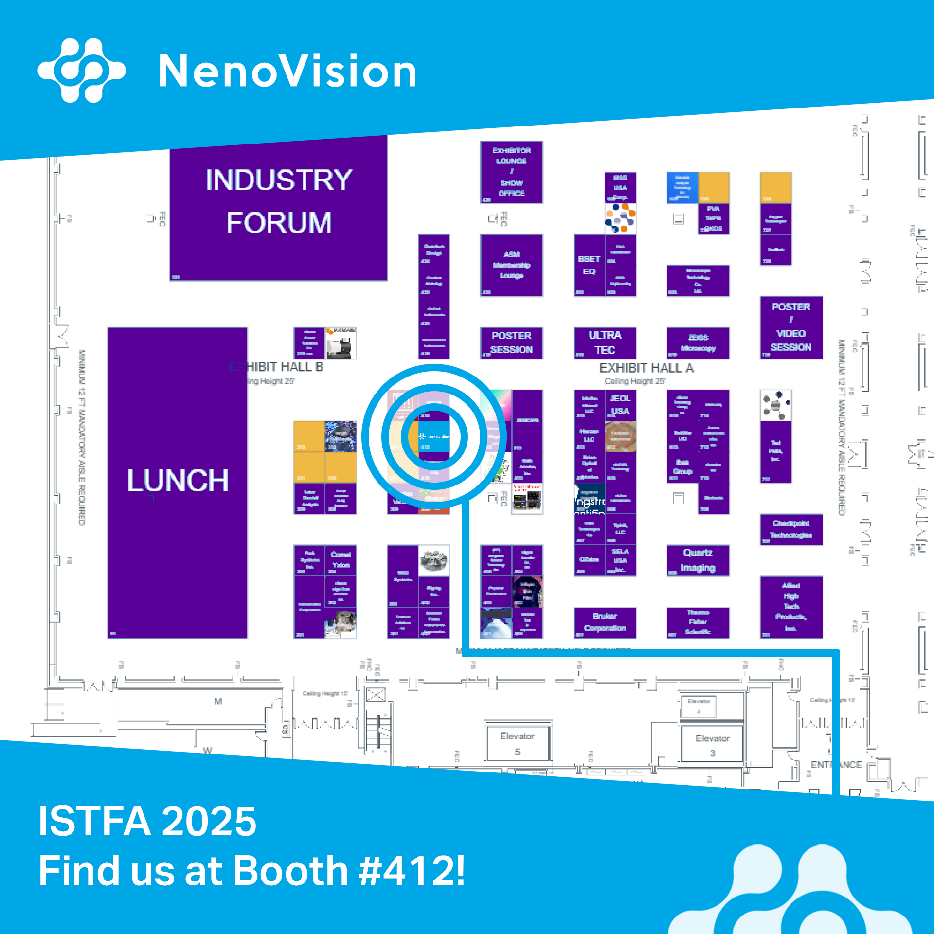
ISTFA 2025

Meet us at ISTFA 2025 in Pasadena, California (November 16-20) - the leading global event for the microelectronics failure analysis community!
|
When?16-20 November 2025 |

|
Where?Pasadena, California, USA |

Where can you find us?
Event
|
09. 10. 2025
|
by Jana Levá
Semiconductors
Product
Technology
Related posts

Product
|
12. 07. 2026
|
by Andrea Karas
LiteScope Phenom now live with Aptco Group
Product

Event
|
25. 06. 2026
|
by Andrea Karas
Where to Meet NenoVision in 2026: Five Conferences Across Three Continents
Technology

Other
|
14. 05. 2026
|
by Andrea Karas
From Brno to Taiwan: LiteScope Meets the Heart of the Semiconductor World
Semiconductors

Event
|
05. 11. 2025
|
by Sabina Žilková
NenoVision has won the Czech Head 2025 award!
Nanostructures
Semiconductors
Product
Technology
Event
|
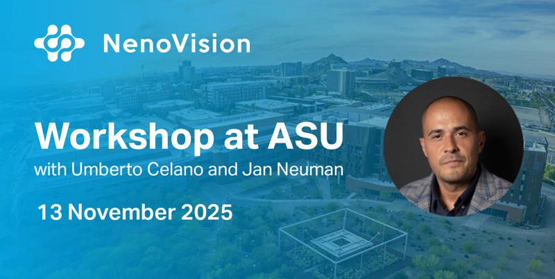
27. 08. 2025
|
by Jana Levá
Workshop at Arizona State University
Semiconductors
Product
Technology