Advancements in graphene nanopatterning using focused electron-beam-induced etching
Researchers strive to unlock the potential of graphene, but precise manipulation remains challenging. In-situ experiments using the AFM-in-SEM LiteScope explore how electron-beam exposure affects SiO2 substrate morphology. Findings reveal subtle effects, guiding the optimization of nanopatterning processes for enhanced graphene-based device development.

Scientific articles
|
28. 02. 2024
|
by Beilstein J. Nanotechnology
Product
Technology
Related articles
Scientific articles
|
17. 12. 2024
|
by ACS Applied Electronic Materials
Impact of Electron Irradiation on WS2 Nanotube Devices
Material Science
Technology
Scientific articles
|
18. 11. 2024
|
by Materials
Enhancing Thermoplastic Starch with Maltodextrin: Key Properties and Performance Insights
Material Science
Technology

Scientific articles
|
12. 08. 2024
|
by Scientific Reports
3D Surface Roughness Measurement of Core–Shell Microparticles
Product
Technology
Scientific articles
|
25. 06. 2024
|
by Production Engineering
ZrN coating as a source for the synthesis of a new hybrid ceramic layer
Product
Technology
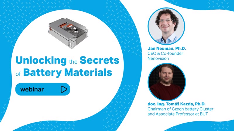
Webinars
|
12. 03. 2024
Unlocking the Secrets of Battery Materials: A Dive into AFM-in-SEM Characterization Webinar
Material Science