LiteScope Helps Localize Defects Invisible to SEM in a Joint Study with NVIDIA

A study presented at ISTFA 2025 by NVIDIA and NenoVision introduces a streamlined approach to semiconductor failure analysis. The work integrates in-situ conductive AFM (CAFM) with plasma FIB in a single SEM platform, making it possible to localize electrical defects that conventional SEM imaging can miss.
In this study ("Streamlined Advanced Semiconductor Failure Analysis Through In-Situ CAFM and Plasma FIB Integration"), Chuan Zhang and Jane Li (NVIDIA), together with Radek Dao and Rosalinda Ring (NenoVision), combined CAFM and plasma FIB into one in-situ workflow. The LiteScope AFM-in-SEM kept the sample under vacuum throughout, removing repeated transfers and vacuum cycles while preserving pristine surfaces for high-quality CAFM imaging. On a stacked-die package, plasma FIB milling handled in-situ delayering and created a grounding path that let CAFM localize leaky gate defects, even where SEM showed no visual defect.
We would like to congratulate the authors, including our colleagues at NVIDIA, on this important contribution to semiconductor failure analysis, and we are proud that LiteScope AFM-in-SEM could support their work.
Read the full paper here:
Related articles

LiteScope Featured in a Nanoscale Study on Back-Contact-Free Electrical AFM

LiteScope Contributes to Study on Creep Behavior and Microstructure Evolution in Advanced Alloys
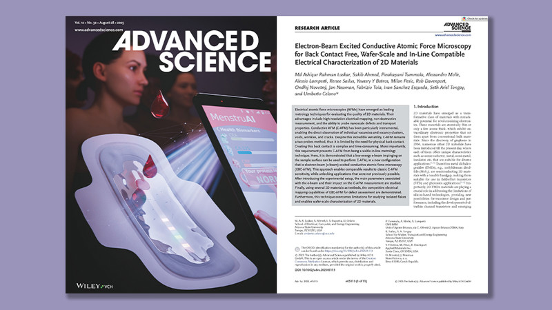
LiteScope Featured in a Breakthrough Study on Electron-Beam-Excited Conductive AFM
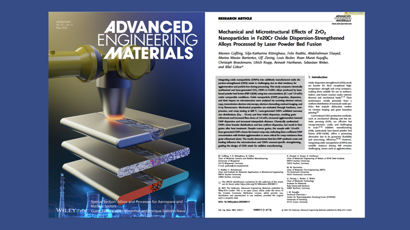
ZrO2 Nanoparticles in Fe20Cr Oxide Dispersion-Strengthened Alloys Processed by Laser Powder Bed Fusion