LiteScope Featured in a Nanoscale Study on Back-Contact-Free Electrical AFM

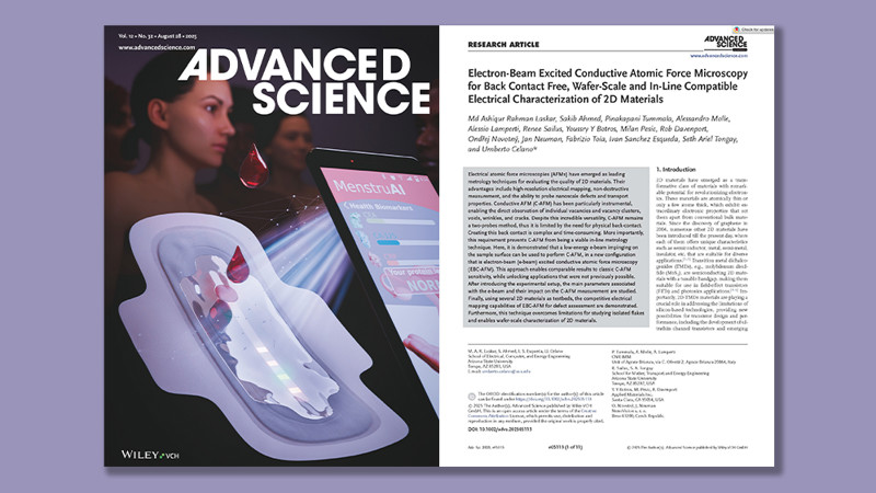
A new study in Nanoscale introduces electron-beam excited AFM (EB-AFM) — a way to run electrical AFM without a physical back-contact. A low-energy electron beam near the AFM probe acts as a remote electrode, removing the destructive sample preparation that conventional conductive AFM requires.
Electrical AFM modes normally need a back-contact to close the circuit, which means cleaving, metallization, or conductive adhesives. That preparation is destructive, works only on small coupon samples, and doesn't fit contamination-controlled, in-line semiconductor metrology. In this study ("Who needs an electrical back-contact after all?"), the team led by Umberto Celano (Arizona State University), with our colleagues Ondřej Novotný and Eduard Jelínek (NenoVision), replaced the back-contact with a focused low-energy electron beam acting as a reconfigurable electrode. They demonstrated contact-free electrical mapping on 2D materials, III–V semiconductors, and fully integrated device structures, reaching defect contrast and sensitivity comparable to conventional methods without modifying the sample.
By removing the back-contact constraint and working at wafer scale, EB-AFM opens a path toward non-destructive, fully automated electrical metrology. We would like to congratulate the authors on this contribution, and we are proud that LiteScope AFM-in-SEM could support their research.
Read the full article here:
Related articles

LiteScope Helps Localize Defects Invisible to SEM in a Joint Study with NVIDIA

LiteScope Contributes to Study on Creep Behavior and Microstructure Evolution in Advanced Alloys
LiteScope Featured in a Breakthrough Study on Electron-Beam-Excited Conductive AFM
ZrO2 Nanoparticles in Fe20Cr Oxide Dispersion-Strengthened Alloys Processed by Laser Powder Bed Fusion