Microscopy is fundamental when working with 2D materials, and the possibility of combining it with AFM opens to a new world of possibilities. Picking up a single flake and being able to measure its thickness saves up time and gives important information at the same time. AFM and SEM combination has advantages that can be exploited in research, but LiteScope has other properties that allow us to make other relevant analysis such as C-AFM, I-V curves, and many other features.

The conventional characterization of 2D materials often necessitates multiple instruments, resulting in challenging and time-consuming localization of regions of interest (ROI). LiteScope, operating within the SEM environment, offers the capability to conveniently localize specific areas, enabling repeatable and comprehensive multimodal analysis. This makes LiteScope an indispensable tool for producing and quality control 2D materials.

Comprehensive in-software analysis provided by NenoView features a three-point plane fit for precise analysis of step-like structures, enhancing its capabilities for in-depth 2D material analysis.
Streamlined Data Management: NenoView's new feature merges multiple measurement files into one, speeding up analysis and simplifying advanced methods for greater efficiency.
Possibility to conduct electrical, mechanical, and piezoelectrical measurements without the need of probe changing, allowing fast multimodal analysis.
The integration of LiteScope inside SEM, combined with the multimodal capabilities of our probes, allows to perform all measurements under the same controlled conditions. This in-situ approach simplifies the analytical process and ensures consistent, reliable results across different modalities.
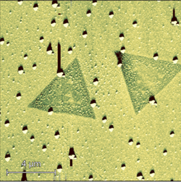
Enabling characterization of 2D materials monolayer.
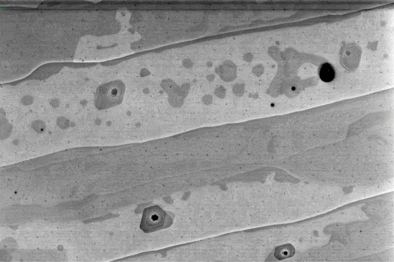
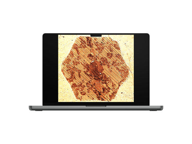
Enabling to analyze large 2D materials flakes in one measurement.
Webinar
Watch our webinar to delve deeper into the key benefits of employing AFM-in-SEM for the characterization of powders, particles, and 2D materials.
- How to effectively measure and determine the surface roughness of powders and particles.
- About the importance of multimodal study of low-dimensional materials for understanding the advanced properties of new functional 2D materials.
- Practical examples from the pharmaceutical and ceramic industries.