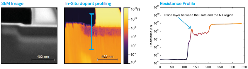
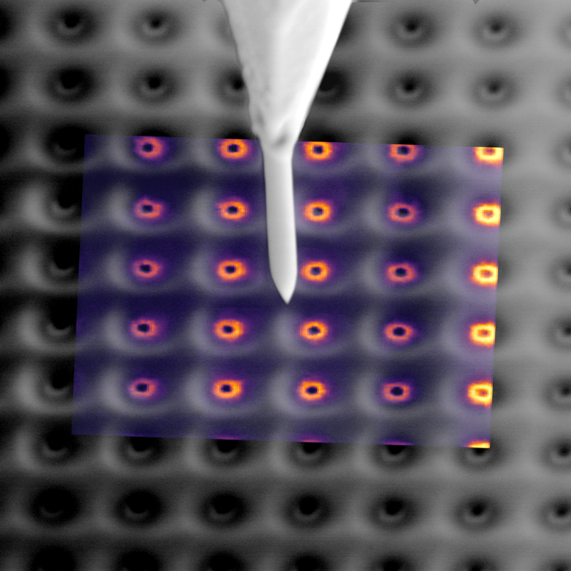
We used LiteScope AFM-in-SEM to perform high-resolution, in-situ electrical characterization of semiconductor devices (MOSFET transistors) through combining Scanning Spreading Resistance Microscopy (SSRM) with SEM imaging to analyze their dopant concentration.
This in-situ SEM-SSRM approach enables efficient mapping of doping profiles at the nanoscale, providing detailed insight into local electrical properties correlated with structural features. It allows precise identification of dopant level variations, which are essential for advanced failure analysis, optimizing device performance, and ensuring long-term reliability.
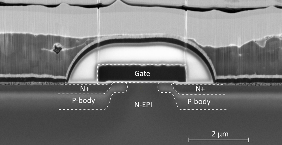
For SiC-based MOSFET transistors, this method facilitates direct analysis of doped layers and junctions, including their geometry, uniformity, and consistency. Understanding the exact shape and positioning of these structures is critical for achieving desired conductivity and minimizing switching and conduction losses in power electronics applications.
Want to discuss your own application ?