"NenoVision represents the best case of developing an idea into a real business in the attractive field of advanced metrology. We are interested in semiconductor applications of correlative microscopy for R&D and production of semiconductor materials and devices, especially wide bandgap structures. NenoVision’s LiteScope AFM-in-SEM has been successfully demonstrated on our silicon carbide samples, and together with its Scanning Spreading Resistance Microscopy (SSRM) mode, it opens up new opportunities in advanced semiconductor analysis."

Navigate directly to specific vias, transistors, or doped layers and perform localized electrical AFM analysis with nanoscale precision.
Perform sample preparation and in-situ analysis within the same vacuum cycle, avoiding surface oxidation or contamination.
Eliminate time-consuming sample transfers and redundant tool usage — streamline failure localization into a single workflow.
„LiteScope empowers us to conduct comprehensive, correlative studies of devices and materials properties while unlocking versatile in-situ ion beam milling and deposition for sample preparation. We're thrilled to be working with the NenoVision team to push the boundaries of this platform and uncover its full potential in the realm of emerging nanoelectronics.“
Nanoelectronics Metrology & Failure Analysis Lab

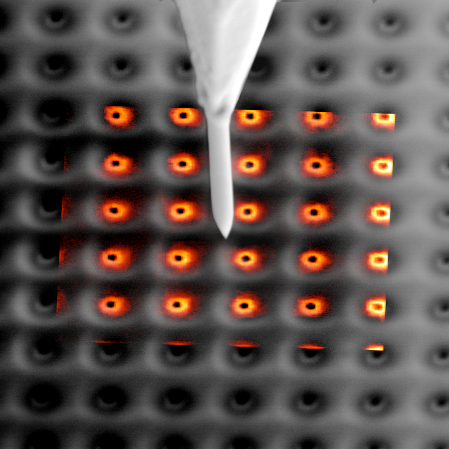
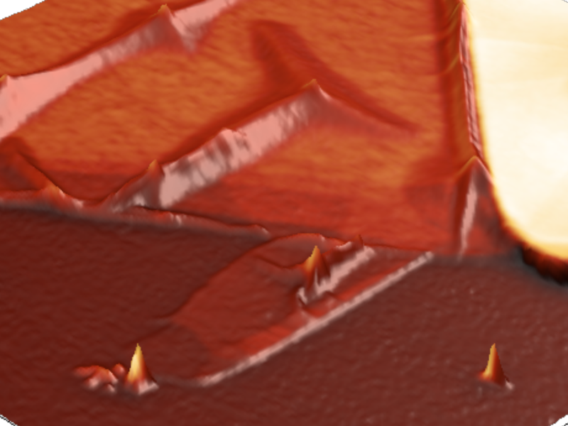
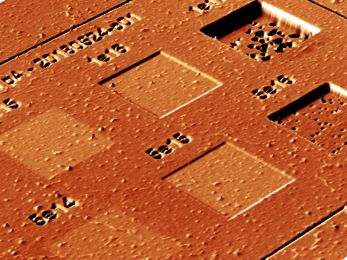
Failure analysis of a NAND structure
We used AFM-in-FIB/SEM to analyze NAND structures, identifying specific vias, sequentially delayering them using PFIB and then characterizing them layer by layer. C-AFM and I/V spectroscopy provide high-resolution electrical characterization, with results correlated to SEM techniques for accurate semiconductor failure analysis. This approach allows for real-time monitoring and reveals electrical failures at various depths of the structure.
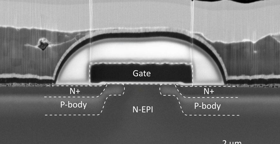
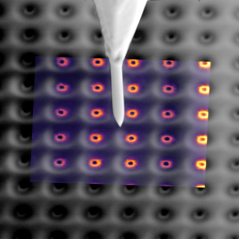
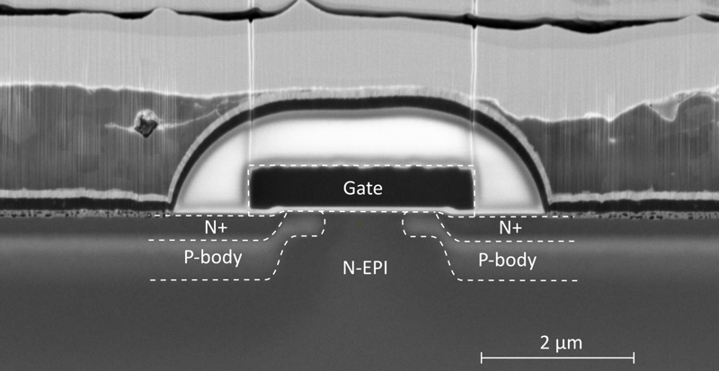
Dopant Concentration Analysis of MOSFET Transistor
SEM-integrated Scanning Spreading Resistance Microscopy (SSRM) was used to map dopant concentration in semiconductor devices (MOSFET Transistor) with nanoscale precision.
In-situ SEM-SSRM approach enables efficient, site-specific electrical characterization of devices by correlating structural imaging with local doping profile, essential for assessing device performance and reliability, enhancing advanced failure analysis.
In SiC MOSFETs, it allows direct analysis of doped layers and junctions, capturing their geometry and uniformity, which is critical for optimizing conductivity and minimizing losses.
Ready to discuss your own application?
Webinar


Inside the Chip: Semiconductor Failure Analysis with AFM-in-SEM

In-Situ SEM Masterclass at QUT University!

Upcoming Battery Webinar | Unveiling Battery Electrode Secrets with AFM-in-SEM